
Lab 7: Introduction to SPI Communication
1. Listening to an SPI “controller”
We will start with a simple example of SPI communication, with the nRF52840 acting as controller (master) and no peripherals (slaves) listening. However, our Analog Discovery 2 will eavesdrop on the communication and this will be our first time to use its Logic app. The nRF52840 will repeatedly transmit one byte containing the value 0xA1 using the code in Program 3.
-
Create a new application.
-
Edit
prj.confto enable both logging and SPI drivers.Program 1. The SPI and logging modules must be enabled inprj.conf.CONFIG_LOG=y CONFIG_SPI=y -
Generate a build configuration and create an overlay.
-
Edit the overlay file.
Program 2. A generic SPI device is specified in the overlay.&i2c0 { status = "disabled";}; (1) &spi0 { status = "disabled";}; &i2c1 { status = "disabled";}; &spi1 { compatible = "nordic,nrf-spim"; status = "okay"; pinctrl-0 = <&spi1_default>; pinctrl-1 = <&spi1_sleep>; pinctrl-names = "default", "sleep"; cs-gpios = <&gpio0 30 GPIO_ACTIVE_LOW>; (2) gendev: gendev@0 { compatible = "vnd,spi-device"; reg = <0>; spi-max-frequency = <125000>; (3) }; }; &pinctrl { spi1_default: spi1_default { group1 { psels = <NRF_PSEL(SPIM_SCK, 0, 28)>, (4) <NRF_PSEL(SPIM_MOSI, 0, 29)>, (5) <NRF_PSEL(SPIM_MISO, 0, 31)>; (6) }; }; spi1_sleep: spi1_sleep { group1 { psels = <NRF_PSEL(SPIM_SCK, 0, 28)>, <NRF_PSEL(SPIM_MOSI, 0, 29)>, <NRF_PSEL(SPIM_MISO, 0, 31)>; low-power-enable; }; }; };1 Unused I2C and SPI controllers are disabled. 2 The chip select pin is set to p0.30. 3 The maximum SPI frequency for this fake device is set to 125 kHz. This is the lowest possible frequency for the nRF52840. 4 The SCK (SPI clock) pin is set to p0.28. 5 The MOSI (master out/slave in) pin is set to p0.29. 6 The MISO (master in/slave out) pin is set to p0.31. -
Enter Program 3 into your
main.c.Program 3. Configure nRF52840 as a SPI controller (master) and transmit 0xA1 repeatedly.#include <zephyr/kernel.h> #include <zephyr/logging/log.h> #include <zephyr/device.h> #include <zephyr/devicetree.h> #include <zephyr/drivers/spi.h> LOG_MODULE_REGISTER(Lab7A, LOG_LEVEL_INF); #define SPIOP SPI_WORD_SET(8) | SPI_TRANSFER_MSB struct spi_dt_spec spispec = SPI_DT_SPEC_GET(DT_NODELABEL(gendev), SPIOP, 0); int main(void) { int err; if (!spi_is_ready_dt(&spispec)) { LOG_ERR("Error: SPI device is not ready."); return -1; } uint8_t tx_buffer[] = {0xA1}; struct spi_buf tx_spi_buf = {.buf = (void*)tx_buffer, .len = sizeof(tx_buffer)}; struct spi_buf_set tx_spi_buf_set = {.buffers = &tx_spi_buf, .count = 1}; err = spi_write_dt(&spispec, &tx_spi_buf_set); LOG_INF("SPI write returns %d", err); while (true) { err = spi_write_dt(&spispec, &tx_spi_buf_set); if (err < 0) { LOG_ERR("spi_write_dt failed. Error = %d", err); return err; } k_usleep(50); } } -
Build your application and flash it to the development board.
-
Convert 0xA1 to binary.
-
Connect a ground flywire to GND on the development board.
-
Connect flywire 0 (pink) to p0.30 on the nRF52840. This is the chip select pin.
-
Connect flywire 1 (green) to p0.28 on the nRF52840. This is the SCK (SPI clock) pin.
-
Connect flywire 2 (purple) to p0.29 on the nRF52840. This is the MOSI (master out/slave in) pin.
-
There is no need to connect anything to p0.31. This is the MISO (master in/slave out) pin and there is no slave to listen to (yet).
-
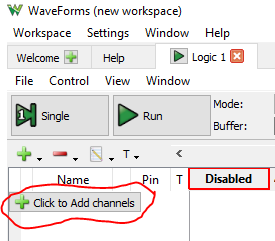
Start Waveforms and launch the Logic app.
-
Click on the green plus sign to add a logic channel to be monitored.
-
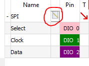
Select SPI for the logic protocol and then change Format to Hexadecimal. If you followed the directions above, then Select (slave select), Clock, and Data (MOSI) should be fine with their defaults.
-
Next, change the Trigger type from Simple to Protocol.

-
Select SPI as the protocol type and then Start as the condition to trigger on.
-
In the Time settings, set Position to 50 us and Base to 20 us/div.
-
Click Single acquisition.
-
Observe the following features:
-
The Select signal is high until the slave is selected by setting it low. It remains low until the end of the transmission.
-
The Clock signal is normally low (as expected for Mode 0 operation). Once the payload is ready to be transmitted the clock signal begins.
-
The Data signal is set to its new value before the Clock signal rises for each bit of the payload. To better see this, change the Base to 1 us/div and click Single again. Notice that you can now that Data changes shortly after the clock signal falls.
-
Set the Base back to 20 us/div and click Single again. Verify that you got the expected binary value (corresponding to 0xA1) by looking at the value of Data at the times that the Clock moved from low to high (as expected for Mode 0 operation).
-
Finally, note that Waveforms has decoded this and displays hA1 above this transmission.
-
-
Sketch the three signals on the worksheet, with downward arrows pointing from the Clock to Data at each of the rising clock transmissions.
-
Modify Program 3 so that SPI is configured for Mode 1 operation. Do this by appending
| SPI_MODE_CPHAto theSPIOPdefinition. -
Run this program and acquire the transmission in the Logic app.
-
You should notice that Logic has not decoded this properly. To fix this, click on the Edit button
and then change Sample to Falling. -
Sketch the three signals on the worksheet. This time put arrows pointing from Clock to Data at each of the falling clock transmissions (as expected for mode 1). Verify the bits of the transmission.
-
Modify Program 3 so that SPI is configured for Mode 3 operation by appending
| SPI_MODE_CPOLto theSPIOPdefinition. -
You should change Sample to Rising for Mode 3.
-
Run this program and acquire the transmission in the Logic app.
-
Sketch the three signals on the worksheet. Notice that in this mode the clock is kept high when off.
-
Draw arrows pointing from Clock to Data at each of the rising clock transmissions (as expected for mode 3).
-
Modify Program 3 so that it is configured for Mode 0 operation (again) and sends two bytes: first 0xA1 and then 0xB7.
-
Run this program and acquire the transmission in the Logic app (with Position set to 100 us).
| Demonstrate that you have successfully sent and decoded this two-byte message. |
2. Interfacing with the ADXL345 accelerometer
The ADXL345 accelerometer can communicate with the nRF52840 via SPI. Your nRF52840 will read acceleration values and then send those to the computer via USB.
-
Create a new application.
-
Edit
prj.confto enable logging (including floating point display) and SPI drivers.Program 4. The SPI and logging modules must be enabled inprj.conf.CONFIG_LOG=y CONFIG_CBPRINTF_FP_SUPPORT=y CONFIG_SPI=y -
Generate a build configuration and create an overlay.
-
Edit the overlay file.
Program 5. The SPI device is configured for an ADXL345 in the overlay.&i2c0 { status = "disabled";}; &spi0 { status = "disabled";}; &i2c1 { status = "disabled";}; &spi1 { compatible = "nordic,nrf-spim"; status = "okay"; pinctrl-0 = <&spi1_default>; pinctrl-1 = <&spi1_sleep>; pinctrl-names = "default", "sleep"; cs-gpios = <&gpio0 30 GPIO_ACTIVE_LOW>; acc: adxl345@0 { compatible = "vnd,spi-device"; reg = <0>; spi-max-frequency = <2000000>; (1) spi-cpol; (2) spi-cpha; (3) }; }; &pinctrl { spi1_default: spi1_default { group1 { psels = <NRF_PSEL(SPIM_SCK, 0, 28)>, <NRF_PSEL(SPIM_MOSI, 0, 29)>, <NRF_PSEL(SPIM_MISO, 0, 31)>; }; }; spi1_sleep: spi1_sleep { group1 { psels = <NRF_PSEL(SPIM_SCK, 0, 28)>, <NRF_PSEL(SPIM_MOSI, 0, 29)>, <NRF_PSEL(SPIM_MISO, 0, 31)>; low-power-enable; }; }; };1 The ADXL345’s default SPI frequency is 2 MHz. 2 The clock polarity is set to 1. 3 The clock phase is set to 1. -
Enter Program 6 into your
main.c.Program 6. Communicate with ADXL345 via SPI/**************************************************************************** Read acceleration from ADXL345 using SPI ADXL345 connections (would normally be part of the README) GND --> ground bus SDO --> p0.31 VCC --> power bus SDA --> p0.29 CS --> p0.30 SCL --> p0.28 *****************************************************************************/ #include <zephyr/kernel.h> #include <zephyr/logging/log.h> #include <zephyr/device.h> #include <zephyr/devicetree.h> #include <zephyr/drivers/spi.h> #define CHILL_TIME 200 LOG_MODULE_REGISTER(Lab7B, LOG_LEVEL_INF); #define SPIOP SPI_WORD_SET(8) | SPI_TRANSFER_MSB struct spi_dt_spec acc = SPI_DT_SPEC_GET(DT_NODELABEL(acc), SPIOP, 0); int main(void) { int err; uint8_t tx_buffer[2]; (1) struct spi_buf config_spi_buf = {.buf = (void*)tx_buffer, .len = sizeof(tx_buffer)}; struct spi_buf_set config_spi_buf_set = {.buffers = &config_spi_buf, .count = 1}; struct spi_buf meas_spi_buf = {.buf = (void*)tx_buffer, .len = 1}; (2) struct spi_buf_set meas_spi_buf_set = {.buffers = &meas_spi_buf, .count = 1}; uint8_t rx_buffer[6]; struct spi_buf rx_spi_buf = {.buf = (void*)rx_buffer, .len = sizeof(rx_buffer)}; struct spi_buf_set rx_spi_buf_set = {.buffers = &rx_spi_buf, .count = 1}; int16_t data[3]; (3) float x,y,z; (4) if (!spi_is_ready_dt(&acc)) { LOG_ERR("Error: SPI device is not ready."); return -1; } // Configure data format tx_buffer[0] = 0x31; // data format register tx_buffer[1] = 0x0B; // set to 16g range err = spi_write_dt(&acc, &config_spi_buf_set); if (err < 0) { LOG_ERR("spi_write_dt failed. Error = %d", err); } k_msleep(CHILL_TIME); (5) // Configure power mode tx_buffer[0] = 0x2D; // power control register tx_buffer[1] = 0x08; // set to measure mode err = spi_write_dt(&acc, &config_spi_buf_set); if (err < 0) { LOG_ERR("spi_write_dt failed. Error = %d", err); } k_msleep(CHILL_TIME); // Read data tx_buffer[0] = 0x32 | 0x40 | 0x80; // read multiple, MB bit high, starting at 0x32 acc.config.operation = acc.config.operation | SPI_HOLD_ON_CS; (6) while (true) { spi_write_dt(&acc, &meas_spi_buf_set); err = spi_read_dt(&acc, &rx_spi_buf_set); spi_release_dt(&acc); (7) if (err < 0) { LOG_ERR("spi_transceive_dt failed. Error = %d", err); } // Combine two bytes to get 16-bit raw acceleration values data[0] = (rx_buffer[1] << 8) | rx_buffer[0]; (8) data[1] = (rx_buffer[3] << 8) | rx_buffer[2]; data[2] = (rx_buffer[5] << 8) | rx_buffer[4]; // Convert raw values to g's (0.004 g/LSB) x = data[0]*0.004; y = data[1]*0.004; z = data[2]*0.004; LOG_INF("x = %f, y = %f, z = %f", x, y, z); k_msleep(CHILL_TIME); } }1 The ADXL345 requires two bytes to configure its registers. The first byte is the register address and the second byte is the value to write to that register. 2 The ADXL345 requires one byte to prepare it to read its registers. The tx_bufferis reused for this purpose, but the length is set to 1.3 The ADXL345 returns 16-bit values for each of the x, y, and z axes. 4 The 16-bit values are converted to g’s using the conversion factor of 0.004 g/LSB. 5 The ADXL345 requires a short delay after configuring its registers. 6 The ADXL345 requires the CS line to be held low between the write and read operations. The SPI_HOLD_ON_CSflag turns off the default behavior of releasing the CS line after each operation.7 The CS line is released after the read operation. 8 The 16-bit values are combined from two bytes. The least significant byte is first in the buffer. The second byte is shifted left 8 bits and then combined with the first byte.
-
Connect the ADXL345 as described in the program header.
-
Create a new project containing Program 6.
-
With the accelerometer resting on the table, verify that you get about 1 g along the z axis and about 0 along the x and y axes.
-
Tilt the accelerometer and observe how the values change.
-
Provide acceleration in various directions and observe the results.
| Demonstrate successful operation of your circuit. |
3. Your Turn
3.1. Tap detection
In this assignment you will demonstrate your ability to use SPI and to extract information from an electronic component data sheet. You will configure an accelerometer to detect single and double taps. Internal nRF52840 LEDs will be used to indicate whether a single tap or a double tap event has occurred.
3.1.1. Project requirements:
-
The majority of your code will be spent configuring the accelerometer prior to putting it into Measure mode and entering a
whileloop. A summary of the configuration commands for the tap features of the ADXL345 appears below, but full details are on the data sheet available from the manufacturer. -
The ADXL345 interrupts will be configured to set INT2 high when either a single or double tap event has occurred. INT2 will be connected to nRF52840 p0.04 (configured as a GPIO).
-
Inside of the
whileloop, you will check to see if the accelerometer has indicated something happened (p0.04 switches from high to low). If it did, you will communicate with the ADXL345 via SPI and determine whether a single or double tap was detected. Note: when a double tap occurs the ADXL345 will also say a single tap occurred (because a double tap consists of at least one tap). We want our single tap indicator to mean that one and only one tap was detected so be careful with the logic. -
It will turn on LED1 if a single tap was detected (but not one that was part of a double tap) and LED2 if a double tap was detected. These will remain lit for 1 second.
3.1.2. Tasks
-
Access the GitHub Classroom link for this assignment on Canvas.
-
Follow the usual steps for getting started with a repository from GitHub Classroom.
-
Your first task is to edit the
Accelerometer-Info-Summary.mdfile in the template project and fill in the missing parts by looking at the ADXL345 data sheet (available through Canvas). -
The configuration of the accelerometer should occur once, outside of the
whileloop. -
Don’t forget to set the power control register to Measure mode as the last step before entering the
whileloop. -
Inside of the
whileloop, your program should check to see if there is an alert on p0.04. If there is, then communicate with the accelerometer and read the interrupt source byte. -
Set the LEDs if a tap has been detected and then keep them on for 1 second.
-
When you are satisfied with its operation, finish documenting your code with comments and a detailed
README.md.
| When your program and circuit are working successfully, remember to push the commits to the remote repository. Also, take a video of its successful operation (along with your reflection) and upload this to Canvas. |